
The TLC272 and TLC277 precision dual operational amplifiers combine a wide range of input offset voltage grades with low offset voltage drift, high input impedance, low noise, and speeds approaching those of general-purpose BiFET devices. These devices use Texas Instruments silicon-gate LinCMOS technology, which provides offset voltage stability far exceeding the stability available with conventional metal-gate processes. The extremely high input impedance, low bias currents, and high slew rates make these cost-effective devices ideal for applications previously reserved for BiFET and NFET products.
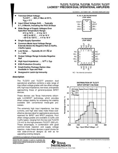
The TLC272, TLC272A, TLC272B, TLC272Y, and TLC277 are LinCMOS™ precision dual operational amplifiers offering low offset voltage, low noise, high input impedance, and single‑supply operation. Various suffixes (C, ‑, M) provide different temperature ranges and performance grades, from the low‑cost TLC272 (10 mV offset) to the high‑precision TLC277 (500 µV offset).\n\nThe document lists absolute maximum ratings, recommended operating conditions, electrical characteristics at 5 V and 10 V supply, and available packaging options such as small‑outline, chip carrier, and tape‑and‑reel. It also includes application information, ESD‑protection details, and an important notice about warranty and product liability.
| Supply voltage (Vpp) range | 3 V to 16 V |
|---|---|
| Input offset voltage (typical) | 10 mV (TLC272) to 500 µV (TLC277) |
| Input bias current (typical) | < 5 pA |
| Packaging options | Small‑outline, chip carrier, tape and reel |
The recommended supply voltage (Vpp) is 3 V to 16 V.
The typical input offset voltage for the TLC277 is 500 µV.