
The ADC12DS105 is a high-performance CMOS analog-to-digital converter capable of converting two analog input signals into 12-bit digital words at rates up to 105 Mega Samples Per Second (MSPS). The digital outputs are serialized and provided on differential LVDS signal pairs. This converter uses a differential, pipelined architecture with digital error correction and an on-chip sample-and-hold circuit to minimize power consumption and the external component count, while providing excellent dynamic performance. The ADC12DS105 may be operated from a single +3.0V or 3.3V power supply. A power-down feature reduces the power consumption to very low levels while still allowing fast wake-up time to full operation. The differential inputs accept a 2V full scale differential input swing. A stable 1.2V internal voltage reference is provided, or the ADC12DS105 can be operated with an external 1.2V reference. The selectable duty cycle stabilizer maintains performance over a wide range of clock duty cycles. A serial interface allows access to the internal registers for full control of the ADC12DS105's functionality.
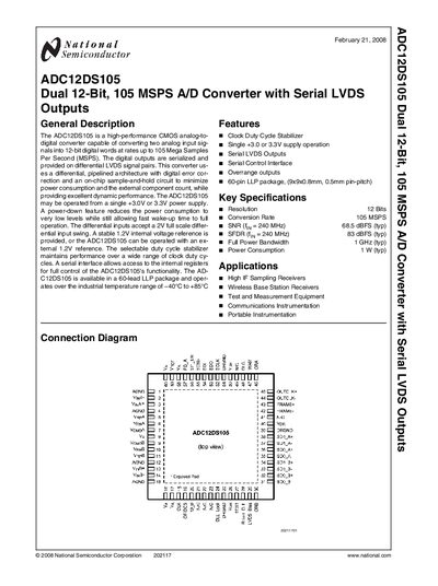
The ADC12DS105 is a high‑performance CMOS analog‑to‑digital converter that converts two analog inputs into 12‑bit digital words at up to 105 MSPS. It operates from a single +3.0 V or 3.3 V supply and includes a differential, pipelined architecture with digital error correction and an on‑chip sample‑and‑hold circuit.
Key features include serial LVDS outputs, a clock duty‑cycle stabilizer, over‑range outputs, and a 60‑lead LLP package. The datasheet provides pin descriptions, electrical characteristics, absolute maximum ratings, and recommended layout guidelines for designers.
| Resolution | 12 Bits |
|---|---|
| Conversion Rate | 105 MSPS |
| Signal‑to‑Noise Ratio (fy = 240 MHz) | 68.5 dBFS (typ) |
| Spurious‑Free Dynamic Range (fy = 240 MHz) | 83 dBFS (typ) |
| Full Power Bandwidth | 1 GHz (typ) |
| Power Consumption | 1 W (typ) |
It can be powered from a single +3.0 V or 3.3 V supply.
The input frequency must be less than 70 MHz.
The device is available in a 60‑lead LLP package.
A 100‑ohm termination resistor should be used on each LVDS pair.