
This document describes the features and characteristics of CD4023BM and CD4025BM, which are buffered triple 3-input NAND gate and buffered triple 3-input NOR gate, respectively. These gates are constructed with complementary metal-oxide-semiconductor (CMOS) integrated circuits, and have equal source and sink current capabilities, conforming to standard B series output drive. The devices also have buffered outputs which improve transfer characteristics by providing very high gain. All inputs are protected against static discharge with diodes to VDD and VSS.
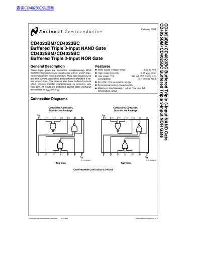
This handbook describes the CD4023 and CD4025 CMOS integrated circuits, which are buffered triple 3‑input NAND and NOR gates. It includes a general description, key features such as a wide 3.0 V‑15 V supply range and high noise immunity, connection diagrams for dual‑in‑line and molded packages, and detailed DC and AC electrical characteristics.
The document also lists absolute maximum ratings, recommended operating conditions, propagation delays, power dissipation limits, and physical dimensions. A life‑support policy disclaimer is provided at the end of the handbook.
| Supply voltage range | 3.0 V to 15 V |
|---|---|
| Power dissipation (dual‑in‑line) | 700 mW |
| Package type | Dual‑In‑Line (J) and Molded Dual‑In‑Line (N) |
The recommended supply voltage is 5 V DC to 15 V DC.
The absolute maximum supply voltage is 0.5 V DC to 18 V DC.
The low‑level output voltage is 0.05 V at VDD = 5 V.