
TI warrants performance of its semiconductor products to the specifications applicable at the time of sale in accordance with TI’s standard warranty.
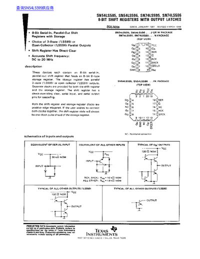
The SN54LS595 is an 8‑bit serial‑in, parallel‑out shift register that includes a D‑type storage register. It is available with either 3‑state outputs (LS595) or open‑collector outputs (LS596) and features separate shift‑register and storage‑register clocks, a direct‑overriding clear, and cascading capability.
The datasheet lists absolute maximum ratings, recommended operating conditions, and detailed electrical parameters such as supply voltage, input/output voltage levels, timing characteristics, and switching behavior. It also contains TI's standard warranty notice and a disclaimer that TI semiconductor products are not intended for life‑support or other critical applications.
| Supply voltage (VCC) | 4.5 V – 6.5 V (typical 5 V) |
|---|---|
| Low‑level input voltage (VIL) | 0.7 V – 0.8 V |
| High‑level output voltage (VOH) | 5.5 V (LS596 only) |
| Low‑level output voltage (VOL) | 0.2 V |
| Shift clock frequency (fSRCK) | up to 20 MHz |
| Setup time SRCK before RCK | 40 ns |
| Hold time SER after SRCK | 7 ns |
The device can operate with a shift clock frequency of up to 20 MHz.
It operates from 4.5 V to 6.5 V, with a typical value of 5 V.