
This document describes an N-Channel MOSFET product that uses high density TrenchFET Gen II power MOSFET technology, with ultra-low on-resistance and optimized Qg. The product also features a new low thermal resistance PowerPAK package with a low profile of 1.07 mm. The product is primarily used in low-side DC/DC conversion, synchronous rectification, and POL applications.
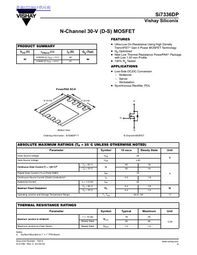
The Si7336DP is a 30‑V N‑channel MOSFET featuring ultra‑low on‑resistance, low gate charge and a compact PowerPAK SO‑8 package. It is intended for low‑side DC/DC conversion, synchronous rectification and other low‑voltage power applications such as notebooks and servers.
The document lists absolute maximum ratings, thermal resistance values, detailed electrical specifications and typical characteristic curves, enabling designers to evaluate the device for their circuits and to ensure safe operating conditions.
| Drain‑Source Voltage (VDS) | 30 V |
|---|---|
| Total Gate Charge (Qg) | 36 nC (typ) / 50 nC (max) |
| Gate Resistance (Rg) | 0.8 Ω (typ) |
| Package | PowerPAK SO‑8, 1.07 mm profile |
The device is rated for a maximum drain‑source voltage of 30 V.
The MOSFET is supplied in a PowerPAK SO‑8 package with a 1.07 mm profile.