
ADP5065 is a fast charge battery manager with power path and USB compatibility from Analog Devices. The product features a 3 MHz switch mode charger, 1.25 A charge current, 500 mA USB host charge current, 4.0 V to 5.5 V operating input voltage, -0.5 V to +20 V (USB VBUS) tolerant input voltage, dead battery isolation FET between battery and charger output, battery thermistor input, and automatic charger shutdown when battery temperature exceeds limits. The product is also compliant with the JEITA Li-Ion battery charging temperature specification and has a SYS_EN_OK flag for holding off system turn-on until the battery is at a minimum required level for guaranteed system startup due to minimum battery voltage and/or minimum battery charge level requirements. Additionally, the product supports C/20, C/10, and specific current level selection of EOC programming.
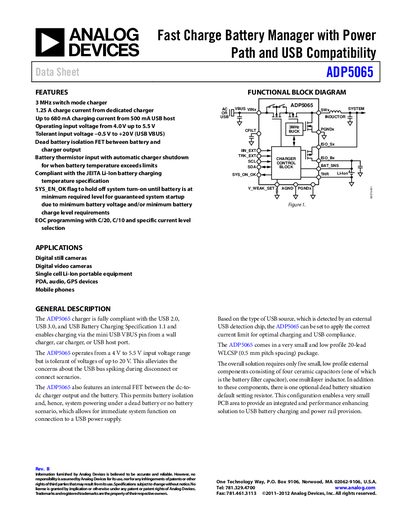
The ADP5065 fast‑charge battery manager complies with USB 2.0, USB 3.0 and the USB Battery Charging Specification 1.1. It can charge from a mini‑USB VBUS pin using wall chargers, car chargers, or USB host ports, operating from 4.0 V to 5.5 V input and tolerating up to 20 V spikes. An internal isolation FET separates the battery from the charger output, allowing system power‑up even with a dead or absent battery.
The device is supplied in a 20‑lead wafer‑level chip‑scale package (0.5 mm pitch) and requires only five external components. It provides programmable charging currents, thermal protection, and I²C‑compatible interface timing, making it suitable for digital cameras, PDAs, GPS devices, mobile phones, and other single‑cell Li‑ion portable equipment.
| Maximum Duty Cycle | 93 % |
|---|---|
| Regulated System Voltage | 3.21 – 3.39 V |
| Battery Termination Voltage | 4.158 – 4.242 V |
| Undervoltage Lockout | 2.25 – 2.45 V |
| Thermal Shutdown Temperature | 140 °C |
The converter’s maximum duty cycle is specified as 93 %.
Thermal early warning triggers at 130 °C and the device shuts down at 140 °C.