
The LTC1155 is a dual high side gate driver that allows the use of low-cost N-channel FETs for high side switching applications. It fully enhances an N-channel MOSFET without the need for external components. Its micropower operation allows use in virtually all systems with maximum efficiency.
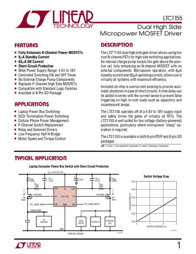
The LTC1155 is a dual high‑side MOSFET driver that fully enhances N‑channel power MOSFETs with very low standby current. It operates from a wide supply range of 4.5 V to 18 V and provides built‑in short‑circuit protection, over‑current sensing, and an internal charge pump to drive the gate above the supply rail.
The document includes absolute maximum ratings, electrical characteristics, pin descriptions, block diagrams, typical performance data, and example application circuits for power‑bus switching, motor control, and relay/solenoid driving. Package options include 8‑lead PDIP, SO, and PLCC formats.
| Supply Voltage (Vs) | 4.5 V – 18 V |
|---|---|
| Input High Voltage (Vinu) | 2.0 V |
| Input Low Voltage (Vine) | 0.8 V |
| Input Capacitance (Cin) | 5 pF |
| Drain Sense Threshold Voltage (Vsen) | 80 mV – 120 mV |
| Turn‑ON Time (Vg=5 V, Cgate=1000 pF) | 50 µs – 250 µs |
The LTC1155 operates from 4.5 V up to 18 V supply voltage.
The internal drain‑sense threshold is between 80 mV and 120 mV.
Yes, the input pins are high‑impedance CMOS gates with ESD protection diodes to ground and supply and must not be forced beyond the power‑rail limits.