
TLC556, TLC556Y DUAL LinCMOS TIMERS are monolithic timing circuits fabricated using the TI LinCMOS process, which provides full compatibility with CMOS, TTL, and MOS logic and operates at frequencies up to 2 MHz.
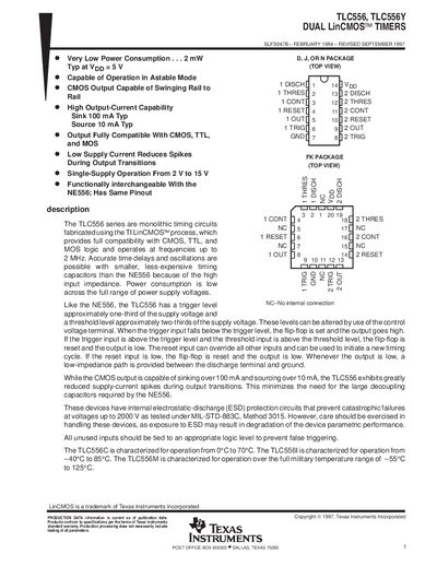
The handbook describes the TLC556 and TLC556Y dual LinCMOS timer integrated circuits, their operation in astable, monostable and bistable modes, and pin‑compatible functionality with the NE556. It highlights low power consumption, high output current capability, and built‑in ESD protection.
Detailed electrical characteristics, absolute maximum ratings, recommended operating conditions, and mechanical dimensions for D, J, N, and FK packages are presented, along with handling and bonding guidelines for the devices.
| Supply voltage range (Vpp) | 2 V to 15 V |
|---|---|
| Input voltage range | -0.3 V to Vpp |
| Operating temperature range (TLC556C) | 0 °C to 70 °C |
| Power dissipation (D package, 25 °C) | 950 mW |
The TLC556 operates from 2 V to 15 V supply voltage.