
The MAX1186 is a 3V, dual 10-bit analog-to-digital converter (ADC) featuring fully-differential wideband track-and-hold (T/H) inputs, driving two pipelined, nine-stage ADCs. The MAX1186 is optimized for low-power, high dynamic performance applications in imaging, instrumentation, and digital communication applications. This ADC operates from a single 2.7V to 3.6V supply, consuming only 105mW while delivering a typical signal-to-noise ratio (SNR) of 59.4dB at an input frequency of 20MHz and a sampling rate of 40Msps. Digital outputs A and B are updated alternating on the rising (CHA) and the falling (CHB) edge of the clock. The T/H driven input stages incorporate 400MHz (-3dB) input amplifiers. The converters may also be operated with single-ended inputs. In addition to low operating power, the MAX1186 features a 2.8mA sleep mode as well as a 1µA power-down mode to conserve power during idle periods. An internal 2.048V precision bandgap reference sets the full-scale range of the ADCs. A flexible reference structure allows the use of this internal or an externally derived reference, if desired for applications requiring increased accuracy or a different input voltage range. The MAX1186 features parallel, multiplexed, CMOS-compatible three-state outputs. The digital output format can be set to two’s complement or straight offset binary through a single control pin. The device provides for a separate output power supply of 1.7V to 3.6V for flexibility.
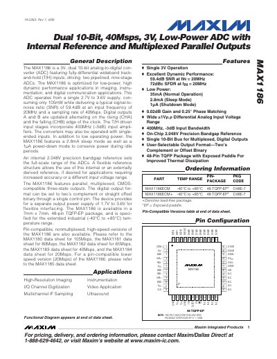
The MAX1186 is a 3 V dual 10‑bit analog‑to‑digital converter designed for low‑power, high‑dynamic‑performance applications. It features fully‑differential wideband track‑and‑hold inputs, a 2.048 V precision bandgap reference, and selectable output formats (two’s complement or offset binary). The device operates from a single 2.7 V to 3.6 V supply and is available in a 48‑pin TQFP‑EP package.
The datasheet provides absolute maximum ratings, detailed electrical characteristics, typical operating curves, pin descriptions, timing specifications, and performance graphs such as SNR, THD, SFDR and bandwidth versus frequency. It also includes reference information for external reference configurations and power‑down modes.
| Supply Voltage Range | 2.7 V to 3.6 V |
|---|---|
| Sampling Rate | 40 Msps |
| Resolution | 10 bits |
| Signal‑to‑Noise Ratio (20 MHz) | 59.4 dB |
| Normal Power Consumption | 35 mA |
| Package | 48‑pin TQFP‑EP, 7 mm × 7 mm |
The device is specified for the extended industrial range of –40 °C to +85 °C.
The digital output format can be set to two’s complement or straight offset binary via a control pin.
The internal precision bandgap reference is 2.048 V.