
TC913A/TC913B is the first monolithic dual auto-zeroed operational amplifier, featuring low power consumption and high precision. It achieves chopper amplifier performance without external capacitors, with low offset voltage and drift characteristics. It can be operated within a wide range of voltages. This product is suitable for applications such as instrumentation, medical instrumentation, embedded control, temperature sensor amplifier, and strain gage amplifier.
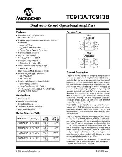
The TC913A and TC913B are dual auto‑zeroed operational amplifiers offering low offset voltage, low noise, and low supply current. Features include a chopper‑stabilized architecture, high DC gain (120 dB), wide common‑mode range, and operation from 3.3 V to 16 V.
The document lists electrical characteristics such as input offset voltage, supply current, bandwidth, and slew rate, as well as pin functions, package dimensions, and typical performance graphs. It also covers overload recovery, latch‑up avoidance, and packaging information for PDIP and SOIC versions.
| Input Offset Voltage (Vos) | 5 µV min, 15 µV typ, 15 µV max (TC913A) |
|---|---|
| Supply Current (Quiescent) | 0.65 mA typ (single supply) |
| Unity‑Gain Bandwidth | 1.5 MHz |
| Slew Rate | 2.5 V/µs |
| CMRR | 116 dB |
| Supply Voltage Range | 6.5 V to 16 V (single supply) |
The TC913A has an input offset voltage of 5 µV minimum, 15 µV typical, and up to 15 µV maximum.
It operates from 6.5 V to 16 V for single‑supply operation.
Typical recovery time from positive output saturation is about 20 ms.
No external capacitors are required; the device uses internal capacitors.