
This document introduces the features and characteristics of a mixed-signal MCU product called C8051F350. The product has a processing capability of 50 MIPS, 8KB Flash memory, 24-bit ADC, and various analog peripherals. These include a 24-bit ADC with 0.0015% nonlinearity, programmable throughput up to 1ksps, 8 external input channels, programmable amplifier gain, etc. Additionally, the product also has a built-in temperature sensor and two 8-bit current DACs. It also provides an internal voltage reference and VDD monitoring/brown-out detection. Furthermore, the product features built-in debug circuitry for full-speed, non-intrusive in-system debugging.
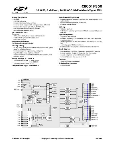
The C8051F350 is a 32‑pin mixed‑signal microcontroller featuring a 50 MIPS 8051 core, 8 kB Flash, 768 bytes RAM, and a 24‑bit ADC with programmable throughput up to 1 ksps. It includes two 8‑bit current‑mode DACs, a comparator with programmable hysteresis, on‑chip debug circuitry, and a range of digital peripherals such as UART, SPI, and SMBus/I²C.
The device operates from 2.7 V to 3.6 V and supports a temperature range of –40 °C to +85 °C. Electrical specifications include a typical active current of 17 mA at 50 MHz, a stop‑mode current below 0.1 pA, and a clock frequency range up to 50 MHz using an internal 24.5 MHz oscillator with a 2× multiplier.
| Supply Voltage | 2.7 V to 3.6 V |
|---|---|
| Typical Operating Current (CPU active, 50 MHz) | 17 mA |
| ADC Resolution | 24 bits |
| ADC Integral Nonlinearity (single‑ended) | +15 ppm FS |
| DAC Resolution | 8 bits |
It operates from –40 °C to +85 °C.
The device is supplied in a 32‑pin lead‑free package.
The ADC can be programmed for a throughput of up to 1 ksps.
Yes, it provides on‑chip debug circuitry with breakpoints, single stepping, and watchpoints.