
This document describes the features and characteristics of the C8051F41x series products, including 12-bit ADC, 12-bit current mode DAC, comparators, POR/Brownout detector, voltage reference, and debugging functionality. The product features a high-speed 8051 microcontroller core and a range of digital peripherals, making it suitable for various applications.
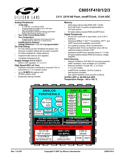
The C8051F410/1/2/3 family combines a high‑speed 8051 core with extensive analog peripherals, including a 12‑bit ADC, two 12‑bit current‑mode DACs, programmable comparators, and an on‑chip temperature sensor. The device operates from 2.0 V to 5.25 V, offers up to 50 MIPS at 50 MHz, and includes on‑chip debug circuitry for in‑system programming and debugging.
The datasheet details memory organization (32 kB or 16 kB Flash, 2.3 kB RAM), digital I/O (24 ports, UART, SPI, SMBus), clock options (internal 24.5 MHz oscillator, external crystal, clock multiplier), and power‑management features such as a programmable LDO regulator and voltage reference. It also provides electrical characteristics, pin‑out diagrams, and register definitions for developers. This manual is written in Chinese.
| Supply Voltage Range | 2.0 V to 5.25 V |
|---|---|
| Flash Memory Size | 32 kB or 16 kB |
| Maximum CPU Throughput | 50 MIPS at 50 MHz |
| Voltage Reference Options | 1.5 V or 2.2 V (programmable) |
The device operates from –40 °C to +85 °C.
It provides either 32 kB or 16 kB of flash memory.
The microcontroller includes hardware SMBus (I²C‑compatible), SPI, and UART ports that can operate concurrently.
Yes, on‑chip debug circuitry allows full‑speed, non‑intrusive debugging without an external emulator.