
MC9S12D-Family is a 16-bit flash-based microcontroller designed for automotive multiplexing applications. It offers fully pin compatible options for different memory and peripheral choices for scalable designs. All MC9S12D-Family members have standard on-chip peripherals, including a 16-bit central processing unit (CPU12), up to 512K bytes of Flash EEPROM, 14K bytes of RAM, 4K bytes of EEPROM, two asynchronous serial communications interfaces (SCI), three serial peripheral interfaces (SPI), IIC-bus, an enhanced capture timer (ECT), two 8-channel 10-bit analog-to-digital converters (ADC), an eight-channel pulse-width modulator (PWM), J1850 interface, and up to five CAN 2.0 A, B software compatible modules (MSCAN12). System resource mapping, clock generation, interrupt control, and bus interfacing are managed by the system integration module (SIM). The MC9S12D-Family has full 16-bit data paths throughout, but the external bus can operate in an 8-bit narrow mode for lower cost systems. The inclusion of a PLL circuit allows power consumption and performance to be adjusted according to operational requirements. In addition to the I/O ports available in each module, up to 22 I/O ports with interrupt capability are available for Wake-Up from STOP or WAIT mode.
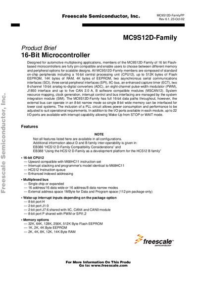
The MC9S12D‑Family is a 16‑bit Flash‑based microcontroller line aimed at automotive multiplexing applications. All members share a 16‑bit CPU12 core, up to 512 KB Flash, up to 14 KB RAM, up to 4 KB EEPROM, and a rich set of on‑chip peripherals including SCI, SPI, I²C, ADCs, PWM, J1850, and up to five CAN 2.0 modules.
The devices are offered in 112‑pin LQFP or 80‑pin QFP packages with configurable I/O, PLL‑based clock generation, and development support such as single‑wire background debug (BDM). Detailed pin‑assignments, memory maps, and package dimensions are provided, and further information can be obtained from www.freescale.com.
| CPU core | 16‑bit CPU12 |
|---|---|
| Flash memory | up to 512 KB |
| SCI interfaces | 2 asynchronous serial communications interfaces |
| SPI interfaces | 3 serial peripheral interfaces |
| ADC modules | 2 × 8‑channel 10‑bit converters |
| PWM channels | 8‑channel pulse‑width modulator |
| CAN modules | up to 5 CAN 2.0 A/B modules |
| Clock generator | Phase‑locked loop multiplier |
| Package types | 112‑Pin LQFP or 80‑Pin QFP |
| Debug support | Single‑wire background debug (BDM) |
The family supports up to 512 KB of Flash EEPROM.
It can accommodate up to five CAN 2.0 A/B software‑compatible modules.
Devices are available in 112‑Pin LQFP and 80‑Pin QFP packages.
A single‑wire background debug (BDM) mode is included.