
The LTC6084/LTC6085 are low cost, low offset, current range 1pA of dual/quad, single-stable output, CMOS operational amplifiers. 1.5MHz gain bandwidth and 0.5V/μs slew rate, as well as the wide supply range and a low 0.75mV offset, make the LTC6084/LTC6085 useful in a wide variety of applications from data acquisition to medical equipment and consumer electronics. The 110μA supply current and the shutdown mode are ideal for signal processing applications which demand performance with minimal power. The LTC6084/LTC6085's output stage swings within 5mV of either supply rail to maximize signal dynamic range in low supply applications. The input common mode range includes the entire supply voltage. These op amps are specified on power supply voltages of 2.5V and 5V from –40°C to 125°C. The dual amplifier LTC6084 is available in 8-lead MSOP and 10-lead DFN packages. The quad amplifier LTC6085 is available in 16-lead SSOP and DFN packages.
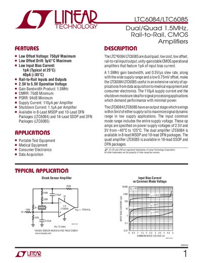
The LTC6084 and LTC6085 are dual/quad CMOS operational amplifiers with rail‑to‑rail inputs and outputs. They offer ultra‑low offset voltage, low offset drift, and extremely low input bias current, making them suitable for portable test equipment, medical devices, and data‑acquisition systems.
The document lists electrical characteristics, absolute maximum ratings, package options, and typical performance curves. It also includes ordering information, recommended solder‑pad layouts, and example applications such as shock‑sensor amplifiers and bipolar analog isolation amplifiers.
| Low Offset Voltage (max) | 750 µV |
|---|---|
| Low Offset Drift (max) | 5 µV/°C |
| Input Bias Current (typical) | 1 pA at 25 °C |
| Input Bias Current (max) | 40 pA < 85 °C |
| Gain Bandwidth Product | 1.5 MHz |
| CMRR (min) | 70 dB |
| PSRR (min) | 94 dB |
| Supply Current (per amplifier) | 110 pA |
| Shutdown Current (per amplifier) | 1.1 pA |
| Operating Voltage Range | 2.5 V to 5.5 V |
The typical input bias current is 1 pA at 25 °C.
The gain‑bandwidth product is 1.5 MHz.