
LTC1051/LTC1053 are high performance, low cost dual/quad zero-drift operational amplifiers. The unique achievement of the LTC1051/LTC1053 is that they integrate on chip the sample-and-hold capacitors usually required externally by other chopper amplifiers. Further, the LTC1051/LTC1053 offer better combined overall DC and AC performance than is available from other chopper stabilized amplifiers with or without internal sample/hold capacitors. The LTC1051/LTC1053 have an offset voltage of 0.5µV, drift of 0.01µV/°C, DC to 10Hz, input noise voltage typically 1.5µVP-P and typical voltage gain of 140dB. The slew rate of 4V/µs and gain bandwidth product of 2.5MHz are achieved with only 1mA of supply current per op amp. Overload recover times from positive and negative saturation conditions are 1.5ms and 3ms respectively, about a 100 or more times improvement over chopper amplifiers using external capacitors. The LTC1051 is available in an 8-lead standard plastic dual-in-line package as well as a 16-pin SW package. The LTC1053 is available in a standard 14-pin plastic package and an 18-pin SO. The LTC1051/LTC1053 are plug in replacements for most standard dual/quad op amps with improved performance.
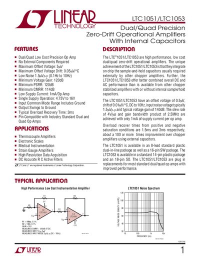
The LTC1051 and LTC1053 are low‑cost, dual‑ or quad‑package zero‑drift operational amplifiers that integrate sample‑and‑hold capacitors on‑chip. They offer ultra‑low offset voltage, low noise, high gain, and low supply current, making them suitable for precision instrumentation, thermocouple amplifiers, and high‑resolution data acquisition.
The document provides detailed electrical characteristics, absolute maximum ratings, package options, typical performance curves, and application notes on achieving picoampere‑level bias currents and minimizing thermal EMF errors. It also includes typical application circuits and recommended layout guidelines.
| Maximum Offset Voltage | 5 µV |
|---|---|
| Maximum Offset Voltage Drift | 0.05 µV/°C |
| Low Noise (0.1 Hz‑10 Hz) | 1.5 µV p‑p |
| Minimum Voltage Gain | 120 dB |
| Minimum PSRR | 120 dB |
| Minimum CMRR | 114 dB |
| Supply Current per Op Amp (no load) | 1 mA |
| Single‑Supply Operating Range | 4.75 V to 16 V |
| Typical Overload Recovery Time | 3 ms |
| Gain‑Bandwidth Product | 2.5 MHz |
| Slew Rate | 4 V/µs |
| Input Capacitance | ≈12 pF |
The typical overload recovery time is 3 ms.
It can operate from a single supply of 4.75 V up to 16 V.
The input offset voltage drift is specified as 0.05 µV/°C.
The gain‑bandwidth product is 2.5 MHz.