
The XC6217 series are precise, low noise, high speed, low dropout regulators with green operation (GO) function. They are fabricated using Torex’s CMOS process. Performance features of the series include high ripple rejection and low dropout voltage, and the series include a reference voltage source, an error amplifier, a current limiter, and a phase compensation circuit. GO provides high speed operation, low power consumption and high efficiencies by automatically switching between a high speed mode (HS) and a power save mode (PS) depending upon the load current level. The switching point of the GO to the output current is being fixed inside the IC. When only high-speed operation is required, it can be fixed by inputting a high level signal to the GO pin, thus providing operating conditions with the most suitable level of supply current for the application. The CE function enables the output to be turned off resulting in greatly reduced power consumption. In this state, with the XC6217B/D series, the IC turns on the internal switch located between the VOUT and VSS pins. This short enables the electric charge at the output capacitor (CL) to be discharged via the internal auto-discharge resistance, and as a result the VOUT pin quickly returns to the VSS level. The series' output stabilization capacitor (CL) is also compatible with low ESR ceramic capacitors.
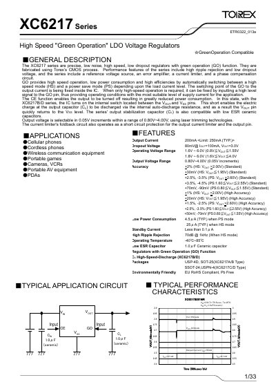
The XC6217 series are precise, low‑noise, high‑speed low‑dropout (LDO) regulators featuring a Green‑Operation (GO) function that automatically switches between high‑speed and power‑save modes to optimise efficiency. They include a reference voltage source, error amplifier, current limiter and phase‑compensation circuit, and are fabricated using Torex’s CMOS process. Typical applications include cellular phones, cordless phones, wireless communication equipment, portable games, cameras, VCRs, portable AV gear and PDAs.
The series supports output voltages from 0.80 V to 4.00 V in 0.05 V steps, with selectable packages (USP‑4D, SOT‑25, SSOT‑24, USPN‑4). Key electrical characteristics such as dropout voltage, ripple rejection, supply current and temperature range are detailed in the parameter tables, and marking rules define the device codes for each variant.
| Output Current (typical) | 200 mA |
|---|---|
| Maximum Output Current | 250 mA |
| Dropout Voltage (typical) | 80 mV @ IOUT=100 mA, VOUT=3.0 V |
| Input Voltage Range | 1.6 V – 6.0 V |
| Output Voltage Range | 0.80 V – 4.00 V (0.05 V steps) |
| Supply Current (standby) | < 0.1 µA |
| Supply Current (power‑save mode) | 4.5 µA (typ.) |
| Ripple Rejection (HS mode) | 70 dB @ 1 kHz |
| Operating Temperature Range | -40 °C – 85 °C |
GO automatically switches the regulator between a high‑speed mode and a power‑save mode based on load current, providing high speed operation with low power consumption.
The output voltage is set by laser‑trimming the internal reference, allowing selection in 0.05 V increments from 0.80 V to 4.00 V.
The series is offered in USP‑4D, SOT‑25, SSOT‑24 and USPN‑4 packages.
The typical output current is 200 mA with a maximum limit of 250 mA.