
This data sheet introduces the TrilithIC's BTS 781 GP product, including power switch, load short circuit protection, over temperature protection, under voltage protection, etc.
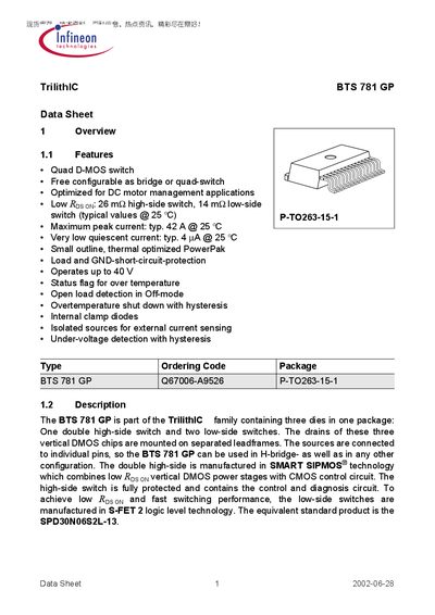
The BTS 781 GP is a quad D‑MOS switch from Infineon's TrilithIC family, offering configurable bridge or quad‑switch operation and optimized for DC motor management. It integrates a high‑side switch with SMART SIPMOS® technology and two low‑side switches using S‑FET 2 logic‑level technology, delivering low on‑resistance and fast switching.
Key features include low Rds(on) values (26 mΩ high‑side, 14 mΩ low‑side), a typical quiescent current of 4 µA, load and GND short‑circuit protection, over‑temperature shutdown, open‑load detection, undervoltage lockout, and internal clamp diodes. The device operates up to 42 V supply voltage and is supplied in a P‑TO263‑15‑1 package.
| Maximum peak current | 42 A (typical at 25 °C) |
|---|---|
| Quiescent current | 4 µA (typical at 25 °C) |
| Operating supply voltage | Up to 42 V |
| Temperature range | -40 °C to 150 °C |
| Status output current | 2 mA |
| ESD protection (high‑side switch) | 1 kV |
The device can operate with a supply voltage up to 42 V.