
Key facts
- Brand
- Infineon
- Model
- BTS 781 GP
- Category
- power switch
- Documents
- 2
- Languages
- EN
- Last added
- 2012-04-05
Start here
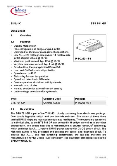
Infineon BTS 781 GP Datasheet
The BTS 781 GP is a quad D‑MOS switch from Infineon's TrilithIC family, offering configurable bridge or quad‑switch operation and optimized for DC motor management. It integrates a high‑side switch with SMART SIPMOS® technology and two low‑side switches using S‑FET 2 logic‑level technology, delivering low on‑resistance and fast switching.
Key features include low Rds(on) values (26 mΩ high‑side, 14 mΩ low‑side), a typical quiescent current of 4 µA, load and GND short‑circuit protection, over‑temperature shutdown, open‑load detection, undervoltage lockout, and internal clamp diodes. The device operates up to 42 V supply voltage and is supplied in a P‑TO263‑15‑1 package.
Infineon BTS 781 GP specifications
| Maximum peak current | 42 A (typical at 25 °C) |
|---|---|
| Quiescent current | 4 µA (typical at 25 °C) |
| Operating supply voltage | Up to 42 V |
| Temperature range | -40 °C to 150 °C |
| Status output current | 2 mA |
| ESD protection (high‑side switch) | 1 kV |
Source: Infineon BTS 781 GP Datasheet
All Infineon BTS 781 GP documents by type
Ratings, dimensions and ordering codes, for selection and design work.
Questions answered in these manuals
What is the maximum supply voltage the device can handle?
The device can operate with a supply voltage up to 42 V.
What is the maximum peak current of the BTS 781 GP?
The device can handle a typical peak current of 42 A at 25 °C.
What are the on‑resistance values for the high‑side and low‑side switches?
The high‑side switch has an on‑resistance of about 26 mΩ, while each low‑side switch is about 14 mΩ (typical at 25 °C).