
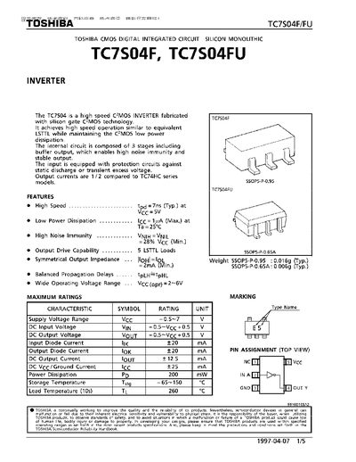
The TC7S04F/FU is a high‑speed CMOS inverter fabricated with silicon‑gate C2MOS technology, offering low power dissipation and high noise immunity. It features a three‑stage internal circuit with a buffered output, static protection against ESD and over‑voltage, and output drive capability of 5 LSTTL loads.
The document lists recommended operating conditions, DC and AC electrical characteristics, pin assignments, and outline drawings for the SSOP5‑P‑0.95 and SSOP5‑P‑0.65A packages, including dimensions and typical weight.
| Supply Voltage Range | 2 V to 6 V |
|---|---|
| Typical Propagation Delay (tpLH) | 7 ns (typ) |
| Output Drive Capability | 5 LSTTL loads |
| Power Dissipation | 200 mW |
| Package Weight (SSOP5‑P‑0.95) | 0.016 g (typ) |
| Input Diode Current | ±20 mA |
The device operates from 2 V to 6 V supply voltage.
The typical tpLH is about 7 ns.
The maximum power dissipation is 200 mW.