
TDA21102 is a dual-channel high-voltage driver chip with fast rise and fall times, strong current absorption, adjustable gate drive voltage, integrated bootstrap diode and other features, suitable for large-power switch power supply and various motor drive circuits
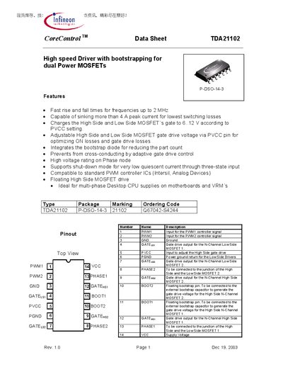
The TDA21102 dual high‑speed driver is designed for half‑bridge circuits that use N‑Channel MOSFETs. It provides fast rise and fall times, low propagation delay, and built‑in protection features, making it suitable for high‑efficiency DC‑DC converters, motor drives, and Class‑D audio applications.
Key specifications include a supply voltage range of 10.8‑13.2 V, adjustable high‑side gate drive (6‑12 V via PVCC), peak sink current over 4 A, and a P‑DSO‑14‑3 package. Thermal resistance is 44.7 K/W (junction‑case) and the device can operate at switching frequencies up to 2 MHz.
| Maximum switching frequency | 2 MHz |
|---|---|
| Peak sink current | >4 A |
| Gate‑drive voltage range (PVCC) | 6‑12 V |
| Package type | P‑DSO‑14‑3 |
| Thermal resistance (junction‑case) | 44.7 K/W |
The driver can sink more than 4 A of peak current.
The PVCC pin allows a gate‑drive voltage of 6 V to 12 V.
It is supplied in a P‑DSO‑14‑3 surface‑mount package.