
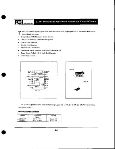
ON Semiconductor TL494 Switchmode Pulse Width Modulation Control Circuits Datasheet


ON Semiconductor TL494 Switchmode Pulse Width Modulation Control Circuits Datasheet - cover page
Brand
FCI
Category
INTEGRATED CIRCUITS
Document type
Datasheet
Language
English
Pages
11
File format
PDF
File size
644 KB
Published
28 March, 2012
Updated
28 March, 2012
Model
TL494
MD5 checksum
16F41D2C8927119AC4917B757A8A7FDD

About this manual

The TL494 is a fixed‑frequency pulse‑width‑modulation controller designed for switch‑mode power supplies. It integrates an on‑chip oscillator, error amplifiers, a 5 V reference and provides both push‑pull and single‑ended output configurations.

The document lists maximum ratings, electrical characteristics, oscillator and dead‑time control sections, and includes typical application schematics, timing diagrams and test‑condition results for designers.

What's inside

  • Maximum Ratings
  • Electrical Characteristics
  • Oscillator Section
  • Error Amplifier Section
  • Dead‑Time Control Section
  • Undervoltage Lockout Section
  • Output Section
  • Timing Diagram
  • Test Conditions Results

Specifications

Power Supply Voltage (VEO) typical15 V
Power Supply Voltage (VEO) maximum42 V
Collector Output Current per transistor500 mA
Reference Voltage (VREF)4.90 V – 5.10 V
Input Offset Voltage (VIO) typical2.0 mV

Frequently asked questions

What is the maximum collector output current for each transistor?

Each output transistor can handle up to 500 mA of collector current.

What is the reference voltage provided by the TL494?

The internal reference voltage is specified as 4.90 V to 5.10 V.

Download PDF (644 KB)

More FCI Manuals


View all FCI manuals →