
This document introduces how to use programmable logic devices as system controllers based on I/O buses
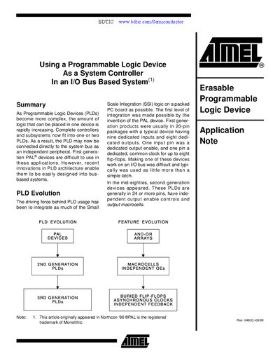
The note describes the evolution of programmable logic devices (PLDs) and highlights the features of third‑generation devices such as the Atmel ATV750. It explains how the ATV750’s extra registers, independent feedback paths, and asynchronous clocks enable the implementation of a peripheral controller/bus interface for an 80186‑based system.
A detailed example shows the ATV750 controlling a custom encryption chip, handling address decoding, data transfer, and status signaling. The document includes logic equations, timing details (8 MHz system clock), and a state‑machine diagram, illustrating how the design fits into a single ATV750 with about 80 % gate utilization.
| Number of flip‑flops | 20 |
|---|---|
| Number of outputs | 10 |
| Maximum gate utilization | ≈80 % of 600 gates |
| Supported clock frequency | 8 MHz |
The ATV750 provides 20 flip‑flops.
The example system uses an 8 MHz clock.
The ATV750 has ten output pins.
The design uses about 80 % of the ATV750’s gate capacity.