
This application note provides guidelines for designing PCBs that mount Atmel’s DataFlash memories in MicroLeadFrame® packages. The MicroLeadFrame package is a leadless package where electrical contact to the PCB is made by soldering the lands on the bottom surface of the package to the PCB, instead of the conventional formed perimeter leads.
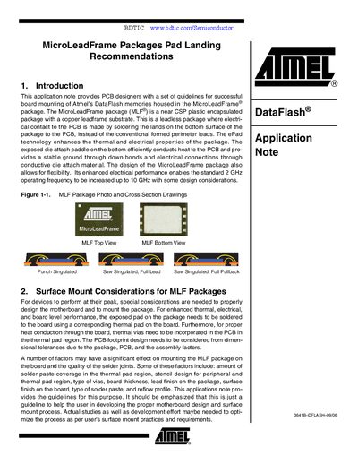
This application note provides PCB designers with guidelines for successful board mounting of Atmel DataFlash memories housed in the MicroLeadFrame (MLF) package. The MLF is a lead‑less, near‑CSP package where the exposed die paddle on the bottom is soldered directly to the PCB, offering improved thermal and electrical performance.
The note covers surface‑mount considerations, PCB pad design, thermal pad and via design, solder‑mask recommendations, stencil design, and rework procedures. It emphasizes the use of NSMD pads for perimeter lands, appropriate thermal via pitch, and specific stencil aperture ratios to achieve reliable solder joints.
| Package body size (6 × 5 × 1.00 mm) | 6 mm × 5 mm × 1.00 mm |
|---|---|
| Package body size (8 × 6 × 1.0 mm) | 8 mm × 6 mm × 1.0 mm |
| Thermal via pitch | 1.0 to 1.2 mm |
| Thermal via diameter | 0.30 to 0.33 mm |
Non‑solder‑mask‑defined (NSMD) pads are recommended for the perimeter lands.
The stencil aperture should have an area ratio greater than 0.66 and an aspect ratio greater than 1.5.
Thermal vias should be placed in an array with a pitch of 1.0‑1.2 mm and a diameter of 0.30‑0.33 mm.
The solder mask opening should be 100 µm smaller than the thermal land size on all four sides.