
This document introduces the characteristics of ADG1334 four independently selectable SPDT switches, including working voltage range, input impedance, input signal range, switch action, etc.
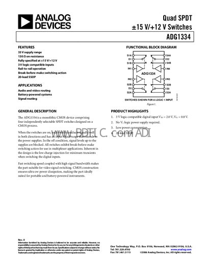
The ADG1334 quad SPDT switch from Analog Devices is a monolithic CMOS device offering four independently selectable switches. It operates from dual supplies (+15 V/‑15 V) or a single 12 V supply, provides rail‑to‑rail operation, and features break‑before‑make switching with low charge injection.
The datasheet includes electrical specifications, pin configurations, functional block diagrams, typical performance curves, absolute maximum ratings, and ordering information for the 20‑lead SSOP package.
| Dual‑supply voltage range | Vop = +15 V, Vss = –15 V |
|---|---|
| Single‑supply voltage | Vop = 12 V, Vss = 0 V |
| Typical on‑resistance (Ron) | 130 Ω |
| Input high voltage (Vint) | 2.0 V min |
| Input low voltage (Vint) | 0.8 V max |
| Turn‑on time (Ton) | 110 ns typical |
| Bandwidth (‑3 dB) | 700 MHz typical |
| Off isolation | 80 dB typical |
| Charge injection | 2 pC typical |
The typical on‑resistance is 130 Ω.
The device uses 3 V logic compatible inputs with a high‑level minimum of 2.0 V and a low‑level maximum of 0.8 V.