
The ADG608/ADG609 are monolithic CMOS analog multiplexers comprising eight single channels and four differential channels respectively, fully specified for ±5 V, +5 V and +3 V power supplies. The ADG608 switches one of eight inputs to a common output as determined by the 3-bit binary address lines A0, A1 and A2. The ADG609 switches one of four differential inputs to a common differential output as determined by the 2-bit binary address lines A0 and A1. An EN input on both devices is used to enable or disable the device. When disabled, all channels are switched OFF. All the address and enable inputs are TTL compatible over the full specified operating temperature range, making the parts suitable for bus-controlled systems such as data acquisition systems, process controls, avionics and ATEs since the TTL compatible address inputs simplify the digital interface design and reduce the board space.
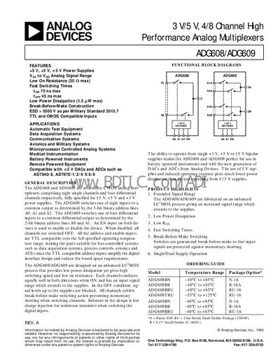
The ADG608 (8‑channel) and ADG609 (4‑channel differential) are monolithic CMOS analog multiplexers designed for +3 V, +5 V or ±5 V supplies. They feature TTL‑compatible address inputs, break‑before‑make switching, low power dissipation and high ESD robustness, making them suitable for data‑acquisition, test equipment, avionics, medical and battery‑powered instruments.
The document provides detailed electrical specifications, ordering information for DIP, SOIC and TSSOP packages, absolute maximum ratings, typical performance curves, test circuit diagrams and mechanical dimensions. It also includes a truth table for channel selection and recommended layout guidelines.
| Analog Signal Range | Vsg to Vpp |
|---|---|
| On‑Resistance (Ron) max | 30 Ω |
| Switching Time (tON) max | 75 ns |
| ESD Rating | >5000 V (MIL‑STD‑3015) |
The maximum on‑resistance is 30 Ω.
They are rated for greater than 5000 V ESD per MIL‑STD‑3015.