
The document describes the features and characteristics of the 16-bit, 500 kSPS PulSAR ADC in MSOP/QFN AD7686 Rev. B. The product features 16-bit resolution with no missing codes, a throughput of 500 kSPS, INL of ±0.6 LSB typical, ±2 LSB maximum, SINAD of 92.5 dB @ 20 kHz, and THD of −110 dB @ 20 kHz. The ADC has a pseudo differential analog input range of 0 V to VREF, supporting VREF up to VDD and no pipeline delay. It operates on a single 5 V supply with 1.8 V/2.5 V/3 V/5 V logic interface, compatible with SPI®-/QSPI™-/MICROWIRE™-/DSP protocols, allowing for daisy-chaining multiple ADCs with a busy indicator. The power dissipation is as low as 3.75 μW @ 5 V/100 SPS, and the standby current is 1 nA. The product is available in a 10-lead MSOP (MSOP-8 size) and 3 mm × 3 mm, 10-lead QFN (LFCSP) (SOT-23 size) package, and it is pin-for-pin compatible with 10-lead MSOP/QFN PulSAR® ADCs.
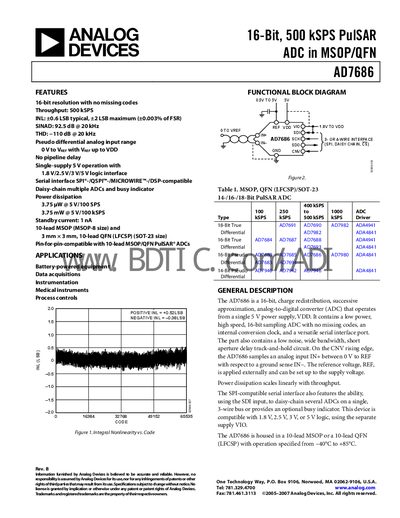
The AD7686 is a 16‑bit, charge‑redistribution successive‑approximation ADC that operates from a single 5 V supply. It offers up to 500 kSPS throughput, a low‑power design (as low as 3.75 pW at 100 SPS), and a versatile SPI‑compatible serial interface that supports daisy‑chaining and optional busy indication. The device includes a low‑noise, wide‑bandwidth track‑and‑hold circuit and supports 1.8 V, 2.5 V, 3 V, or 5 V logic levels.
Typical applications include battery‑powered data acquisition, instrumentation, medical devices, and process control. The AD7686 is available in 10‑lead MSOP or QFN (LFCSP) packages and operates over a temperature range of –40 °C to +85 °C.
| Resolution | 16 bits |
|---|---|
| Maximum Throughput | 500 kSPS |
| Supply Voltage (VDD) | 4.5 V to 5.5 V |
| Operating Temperature Range | -40 °C to +85 °C |
| Standby Current | 1 nA |
| Power Dissipation (typical, 5 V, 100 kSPS) | 3.75 mW |
| Logic Interface Levels | 1.8 V, 2.5 V, 3 V, or 5 V |
The AD7686 can sample up to 500 kSPS.
It operates with a VDD of 4.5 V to 5.5 V.
Yes, it supports 1.8 V, 2.5 V, 3 V, or 5 V logic levels via the VIO pin.
The standby current is 1 nA.