
The DS2188 T1/CEPT Jitter Attenuator Chip is capable of attenuating clock and data jitter present in T1 or CEPT lines. It meets the jitter attenuation templates outlined in TR62411, TR-TSY-000170, G.735, and G.742. Only one external component, either a 6.176 MHz (T1) or 8.192 MHz (CEPT) crystal, is required. The buffer size can be selected as 128 or 32 bits. Jitter attenuation can be easily disabled. It operates on a single +5V supply using low-power CMOS technology. The DS2188 is available in 16-pin DIP and 16-pin SOIC (DS2188S) packages. It is designed to work with the DS2186 Transmit Line and DS2187 Receive Line Interface.
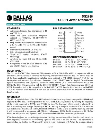
The DS2188 is a T1/CEPT jitter attenuator that uses a 128 × 2‑bit FIFO buffer and an external 4× crystal to reduce clock and data jitter. It operates from a single +5 V supply and supports selectable buffer depths of 128 or 32 bits.
The document provides pin descriptions, recommended crystal parameters, absolute maximum ratings, DC and AC electrical characteristics, and package dimensions for both 16‑pin DIP and SOIC versions.
| Buffer depth selectable | 128 bits or 32 bits via BDS pin |
|---|---|
| Supply voltage (Vpp) | 5.0 V (typical) |
| Input logic high (Vin) | 2.0 V (typical) |
| Input logic low (Vin) | -0.3 V to +0.8 V |
| Supply current (Ipp) | 7 mA to 12 mA |
| Crystal frequency | 6.176 MHz (T1) or 8.192 MHz (CEPT) |
| Load capacitance | 14 pF to 20 pF (16 pF preferred) |
| Effective series resistance (ESR) max | 40 Ω (6.176 MHz) / 30 Ω (8.192 MHz) |
Tie the DJA pin high to bypass the jitter attenuator and pass the raw signals through.
The BL pin goes high when the buffer is near full or empty, signalling that incoming jitter exceeds the allowed limit (120 UIpp for 128‑bit mode, 28 UIpp for 32‑bit mode).
Apply a negative‑edge (high‑to‑low) transition on the RST pin; this recenters the FIFO buffer.