
The XC9110/9111 series is a group of PFM controlled step-up DC/DC converter/controller ICs designed to generate low supply voltage by the combination of PFM control and CMOS structure. The series is ideal for applications where a longer battery life is needed such as in portable communication equipment. With a built-in 2.5ΩN-channel driver transistor, the XC9110A/C/E and XC9111A/C/E types provide a step-up operation by using only a coil, a capacitor, and a diode connected externally. The XC9110/9111B, D and F versions can be used with an external transistor for applications requiring larger currents. Output voltage is internally programmable in a range from 1.5V to 7.0V in increments of 0.1V (accuracy:±2.5%). Maximum oscillation frequency is set to 100kHz for XC9110/9111 series. (At light loads, it is set to 180kHz for the XC9111 series.) Options include products equipped with a CE pin (C and D versions) that allows the IC to be shut down thereby reducing supply current and with separated VDD/VOUT pins (E and F versions) to separate the power supply block and the output voltage detect block. With the XC9110 series, maximum duty cycle is set to 75% (VDD=3.3V) making it suitable for use with large current operations. The XC9111 series automatically switches duty ratio between 56% & 75% (VDD=3.3V) when it senses changes in load to drop output ripple voltage and can support both
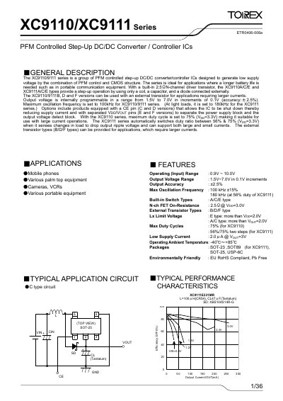
The XC9110/XC9111 series are PFM‑controlled step‑up DC/DC converter/controller ICs designed for low‑power portable applications such as mobile phones, palm‑top equipment, cameras and other portable devices. They generate a low supply voltage from a wide input range and include built‑in N‑channel MOSFET drivers.
Key features include an input range of 0.9 V‑10 V, programmable output from 1.5 V to 7.0 V in 0.1 V steps, ±2.5 % accuracy, duty‑cycle control (75 % for XC9110, 56 %‑75 % for XC9111), low supply current (2 µA), and operation from –40 °C to +85 °C. Available in SOT‑23, SOT‑89, SOT‑25 and USP‑6C packages.
| Operating Input Range | 0.9 V ~ 10.0 V |
|---|---|
| Output Voltage Range | 1.5 V – 7.0 V (0.1 V steps) |
| Output Accuracy | ±2.5 % |
| Maximum Oscillation Frequency | 100 kHz ±15 % (180 kHz at 56 % duty for XC9111) |
| Built‑in Switch Type | N‑channel FET (A/C/E types) |
| Maximum Duty Cycle | 75 % (XC9110) / 56 %‑75 % (XC9111) |
| Low Supply Current | 2.0 µA @ VOUT=3 V |
| Operating Ambient Temperature | -40 °C to +85 °C |
| Package Types | SOT‑23, SOT‑89, SOT‑25, USP‑6C |
The output voltage can be programmed from 1.5 V to 7.0 V in 0.1 V increments.
The XC9110 series operates with a maximum duty cycle of 75 % (VDD = 3.3 V).
The device draws a low supply current of 2.0 µA when VOUT is 3 V.
They are offered in SOT‑23, SOT‑89, SOT‑25, and USP‑6C packages.