
The LTC1411 is a 2.5Msps sampling 14-bit A/D converter in a 36-pin SSOP package, which typically dissipates only 195mW from a single 5V supply. This device comes complete with a high bandwidth sample-and-hold, a precision reference, programmable input ranges and an internally trimmed clock. The ADC can be powered down with either the Nap or Sleep mode for low power applications. The LTC1411 converts either differential or single-ended inputs and presents data in 2’s complement format. Maximum DC specs include ±2LSB INL and 14-bit no missing code over temperature. Outstanding dynamic performance includes 80dB S/(N + D) and 90dB THD at 100kHz input frequency. The LTC1411 has four programmable input ranges selected by two digital input pins, PGA0 and PGA1. This provides input spans of ±1.8V, ±1.27V, ±0.9V and ±0.64V. An out-of-the-range signal together with the D13 (MSB) will indicate whether a signal is over or under the ADC’s input range. A simple conversion start input and a data ready signal ease connections to FIFOs, DSPs and microprocessors.
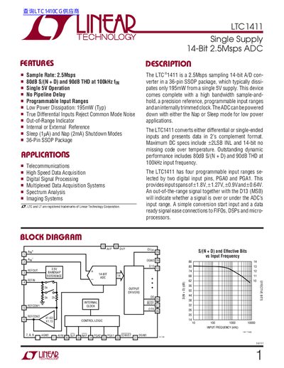
The LTC1411 is a 14‑bit analog‑to‑digital converter that operates from a single 5 V supply and samples at up to 2.5 Msps. It offers four programmable input ranges (+1.8 V, +1.27 V, +0.9 V, +0.64 V), true differential inputs, low power dissipation (195 mW typ), and sleep/nap shutdown modes.
The datasheet details pin functions, timing characteristics, typical performance graphs, and example applications such as telecommunications, high‑speed data acquisition, and imaging systems. It also provides ordering information, absolute maximum ratings, and reference circuitry for designers.
| Sample Rate | 2.5 Msps |
|---|---|
| Resolution | 14 bits |
| Power Dissipation (typ) | 195 mW |
| Signal‑to‑Noise Ratio (100 kHz) | 80 dB |
| Total Harmonic Distortion (100 kHz) | -90 dB |
The LTC1411 can sample at up to 2.5 Msps.
The device has a Nap mode (≈2 mA) and a Sleep mode (≈1 pA).
Typical power dissipation is 195 mW.