
This is a cost-effective solution for multi-service access applications. It is especially suited for ADSL, VDSL, FTTx and HFC applications, where all services are transported over ATM.
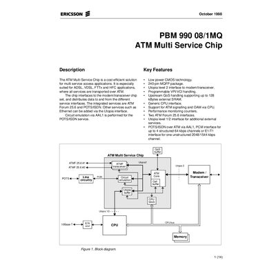
The PBM 990 08/1MQ ATM Multi Service Chip is a low‑power CMOS solution for multi‑service access applications such as ADSL, VDSL, FTTx and HFC. It integrates two ATM Forum 25.6 interfaces, a PCM/E1/T1 telephony service, and a programmable Utopia level‑2 interface for modem/transceiver connectivity. QoS buffering is provided by up to 128 kBytes of external SRAM, and the chip supports ATM signalling, OAM and performance monitoring counters.
The chip offers a generic CPU interface with a 16‑bit bidirectional bus, interrupt signaling, and separate upstream/downstream buffers. Clock requirements include a system clock of 16‑32 MHz, a 32 MHz ATMF clock, and an 8 kHz network reference clock for timing insertion. All functions are hardware‑implemented, allowing high bandwidth handling in both downstream and upstream directions.
| Technology | Low power CMOS |
|---|---|
| Package | 240‑pin MQFP |
| Modem/Transceiver Interface | Utopia level 2 |
| VPI/VCI Handling | Programmable |
| External SRAM for QoS | Up to 128 kBytes |
| ATM Forum Interfaces | Two 25.6 Mbps interfaces |
| ATM Signalling & OAM | Supported via CPU |
| Performance Counters | Various (downstream/upstream cell, EPD, PPD) |
The chip supports up to 128 kBytes of external SRAM for QoS buffering.
Two ATM Forum 25.6 Mbps interfaces are provided.
A Utopia level‑2 interface connects the chip to the modem/transceiver.