
74LCX373 is a low voltage CMOS OCTAL D-TYPE LATCH with 3 STATE OUTPUT NON-INVERTING fabricated with sub-micron silicon gate and double-layer metal wiring C2MOS technology. It is ideal for low power and high speed 3.3V applications; it can be interfaced to 5V signal environment for both inputs and outputs. These 8 bit D-Type latch are controlled by a latch enable input (LE) and an output enable input (OE). While the LE inputs is held at a high level, the Q outputs will follow the data input. When the LE is taken low, the Q outputs will be latched precisely at the logic level of D input data. While the (OE) input is low, the 8 outputs will be in a normal logic state (high or low logic level) and while (OE) is in high level, the outputs will be in a high impedance state. It has same speed performance at 3.3V than 5V AC/ACT family, combined with a lower power consumption. All inputs and outputs are equipped with protection circuits against static current damage.
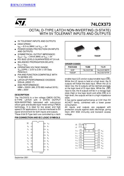
The 74LCX373 is a low‑voltage CMOS octal D‑type latch with non‑inverting 3‑state outputs, compatible with the 74 series 373. It features 5 V tolerant inputs and outputs, symmetrical output impedance, and built‑in ESD protection.
The device operates from 2.0 V to 3.6 V, provides up to 24 mA output drive, and exhibits propagation delays around 8 ns. It is offered in SOP‑20 and TSSOP‑20 packages with detailed mechanical dimensions provided.
| Supply Voltage Range | 2.0 V to 3.6 V |
|---|---|
| Output Drive Current (3.0‑3.6 V) | +24 mA |
| Propagation Delay (max) | 8.0 ns |
| ESD Protection (HBM) | >2000 V |
| Storage Temperature | -65 °C to +150 °C |
It operates from 2.0 V to 3.6 V.
The device offers HBM protection greater than 2000 V and MM protection greater than 200 V.
The maximum propagation delay is 8.0 ns at a supply voltage of 8 V.
It is available in SOP‑20 (order code 74LCX373M) and TSSOP‑20 (order code 74LCX373T) packages.