
This document describes the features and characteristics of the 74V1T125 SINGLE BUS BUFFER, including high speed performance, low power dissipation, compatibility with TTL outputs, power down protection on inputs and outputs, and protection against static discharge and transient excess voltage.
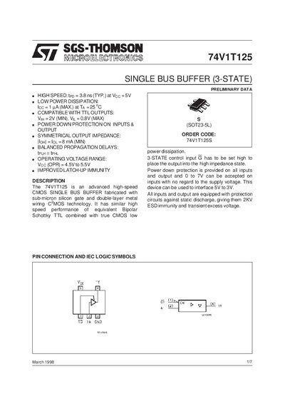
The 74V1T125 is a high‑speed CMOS single‑bus buffer with low power dissipation and TTL‑compatible inputs. It features a typical propagation delay of 3.8 ns, symmetrical output impedance, and built‑in power‑down protection.
The document lists absolute maximum ratings, recommended operating conditions, DC and AC electrical specifications, capacitance values, and mechanical dimensions for the SOT23‑5L package. Test circuit diagrams and timing waveforms illustrate propagation delays and enable/disable times.
| Operating Voltage Range (Vcc) | 4.5 V to 5.5 V |
|---|---|
| Input Capacitance (Cin) | 4 pF |
| Output Capacitance (Cout) | 10 pF |
| Operating Temperature Range | -40 °C to +85 °C |
The device is specified to operate with a supply voltage between 4.5 V and 5.5 V.
The part is supplied in an SOT23‑5L surface‑mount package.