
This document introduces a system approach for designing high performance bootstrap gate driver circuits for power MOSFETs and IGBTs, in high-frequency, high-power, and high efficiency switch applications. Different experience electrical engineers can benefit from it.
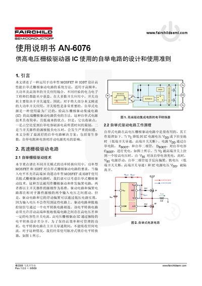
This document provides an introduction to bootstrap gate‑driver circuits for high‑voltage MOSFET and IGBT applications. It explains the operating principle, advantages, and the main limitations such as duty‑cycle constraints and negative‑voltage issues on the Vs pin.
The note then details the design process for bootstrap components, including selection of bootstrap capacitors and resistors, various circuit topologies, and considerations for HVIC current capability and gate‑resistance design. Practical equations and example values are given to aid engineers in creating reliable high‑voltage driver circuits. This manual is written in Chinese.
| Bootstrap supply voltage (Vpp) | 15 V |
|---|---|
| Recommended bootstrap capacitor range | 100 nF – 570 nF |
| Bootstrap resistor typical range | 5 Ω – 108 Ω |
The duty cycle is limited by the time required to recharge the bootstrap capacitor.