
Key facts
- Brand
- GSI
- Model
- GS100
- Industry
- Industrial
- Documents
- 4
- Languages
- EN
- Last added
- 2012-06-07
Start here
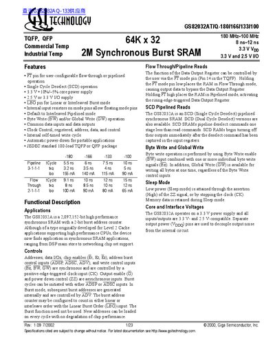
GSI TECHNOLOGY GS82032AT/Q-180/166/133/100 64K x 32 2M Synchronous Burst SRAM
The GS82032A is a 64K x 32-bit (2M bit) high-performance synchronous SRAM designed for applications ranging from DSP main stores to networking chipset support. It features a 2-bit burst address counter that can be configured for linear or interleaved burst modes via the LBO pin.
The device operates with a 3.3V core power supply and supports 2.5V or 3.3V I/O voltages. Key operating frequencies include 180 MHz, 166 MHz, 133 MHz, and 100 MHz. The chip includes user-configurable flow-through or pipelined operation via the FT pin and offers single-cycle deselect (SCD) functionality.
GSI GS100 specifications
| Memory Capacity | 64K x 32 (2M bits) |
|---|---|
| Operating Frequency | 180 MHz - 100 MHz |
| Access Time | 8 ns - 12 ns |
| Core Voltage | 3.3 V (+/- tolerance) |
| I/O Voltage | 2.5 V or 3.3 V |
| Package Type | TQFP, QFP (100-lead) |
Source: GSI TECHNOLOGY GS82032AT/Q-180/166/133/100 64K x 32 2M Synchronous Burst SRAM
All GSI GS100 documents by type
Ratings, dimensions and ordering codes, for selection and design work.
- GSI TECHNOLOGY GS82032AT/Q-180/166/133/100 64K x 32 2M Synchronous Burst SRAM 23 p
- GSI TECHNOLOGY GS842Z18/36AB-180/166/150/100 Manual 31 p
- GSI TECHNOLOGY GS840Z18/36AT-180/166/150/100 4Mb Pipelined Flow Through Synchronous NBT SRAMs handbook 24 p
- GSI Technology GS84018/32/36AT/IB-190/180/166/150/100 4Mb Sync Burst SRAM Datasheet 31 p
Questions answered in these manuals
What are the available operating frequencies for this SRAM?
The device is available in versions operating at 180 MHz, 166 MHz, 133 MHz, and 100 MHz.
From: GSI TECHNOLOGY GS82032AT/Q-180/166/133/100 64K x 32 2M Synchronous Burst SRAM
Can the burst order be configured?
Yes, the Burst address counter may be configured to count in either linear or interleaved order with the Linear Burst Order (LBO) input.
From: GSI TECHNOLOGY GS82032AT/Q-180/166/133/100 64K x 32 2M Synchronous Burst SRAM
What supply voltages does the GS842Z18/36AB support?
It uses a 3.3 V core supply with ±10 % tolerance and can be powered with either 2.5 V or 3.3 V Vpp for the I/O pins.
What package is the GS842Z18/36AB offered in?
The device is supplied in a JEDEC‑standard 119‑bump BGA package that is RoHS‑compliant.
What operating modes does the GS840Z18/36AT support?
It can be configured by the user to operate in either Pipeline mode or Flow‑Through mode, both providing NBT functionality.
How is power‑down controlled on the device?
The ZZ pin provides automatic power‑down when asserted high.