
This is a design manual for the DC1789A product, which is an isolated USB transceiver based on LTM®2884, with isolated power. It has an EMI optimized circuit configuration and printed circuit board layout.
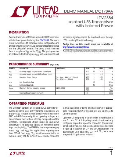
This document provides setup and operating instructions for the DC1789A demonstration circuit, which features the LT M®2884 isolated USB transceiver. The circuit includes an isolated DC/DC converter delivering 5V to VCC2 and supports USB signaling across an isolation barrier. It operates from VCC and/or VBUS supplies, with configurable power modes and EMI-optimized layout. The manual includes quick start procedures, PCB layout, parts list, and safety warnings for engineering evaluation use only.
The circuit supports low-speed (1.5 Mbps) and full-speed (12 Mbps) USB data rates, with integrated pull-up and pull-down resistors. It includes a suspend power feature to reduce current during idle USB bus conditions. EMI performance is optimized with minimized ground plane size and signal loop reduction. The document also includes schematic diagrams, component details, and important safety and compliance disclaimers.
| Operating Supply Range (VCC) | 4.4V to 16.5V |
|---|---|
| Operating Supply Range (VBUS) | 4.4V to 16.5V |
| Regulated Output Voltage (VCC2) | 4.75V to 5.25V |
| Low Speed Data Rate | 1.5 Mbps |
| Full Speed Data Rate | 12 Mbps |
| Maximum Working Insulation Voltage | 400VDC |
VCC operates from 4.4V to 16.5V, and VBUS operates from 4.4V to 16.5V.
The regulated output voltage is 4.75V to 5.25V, depending on input conditions.
It supports 1.5 Mbps for low-speed devices and 12 Mbps for full-speed devices.
The maximum working insulation voltage is 400VDC.