
This document describes the features and characteristics of the Analog Devices operational amplifier product ADA4661-2, including low power consumption under high voltage, low offset voltage, etc.
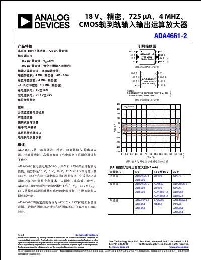
The document describes the ADA4661-2, a dual-channel, precision, rail-to-rail input/output (I/O) operational amplifier optimized for low-power, high-bandwidth, and wide supply voltage applications. It features low offset voltage, low bias current, and operates with single supplies from 3 V to 18 V or dual supplies from ±1.5 V to ±9 V.
The datasheet details performance characteristics across three specific supply voltages: 18 V, 10 V, and 3.0 V. It includes absolute maximum ratings, thermal resistance data, pin configurations, typical performance curves, and comprehensive application notes covering topics such as input stages, gain stages, output stages, capacitive load driving, and EMI suppression ratios. This manual is written in Chinese.
| Supply Voltage Range (Single) | 3 V to 18 V |
|---|---|
| Supply Voltage Range (Dual) | ±1.5 V to ±9 V |
| Lowest Supply Current | 725 µA (max) |
| Offset Voltage (Typical, VSY/2) | 150 µV |
| Input Bias Current (Max, -40°C to +85°C) | 15 pA |
| Gain Bandwidth Product | 4 MHz (typical, AV = 100) |
| Unity-Gain Bandwidth | 4 MHz |
| -3 dB Closed-Loop Bandwidth | 2.1 MHz (typical) |
The device has an extended industrial temperature range of −40°C to +125°C.
The device is available in 8-pin MSOP and 8-pin LFCSP (3 mm x 3 mm) packages.
Yes, the device is unity-gain stable.