
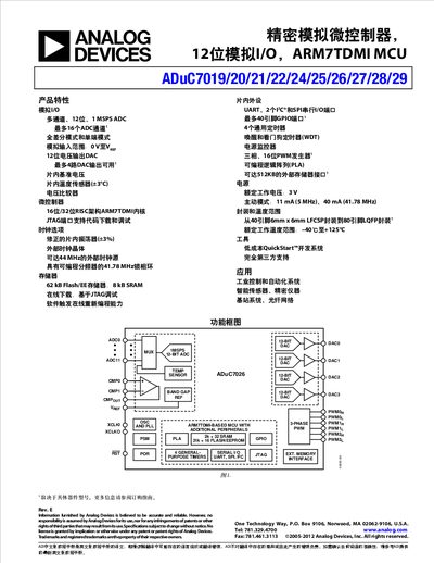
The ADuC7019/20/21/22/24/25/26/27/28/29 family integrates a 12‑bit, up‑to‑1 MSPS ADC, up to four 12‑bit DACs, a 41.78 MHz ARM7TDMI® core, 62 kB Flash/EE and 8 kB SRAM on a single chip. It includes on‑chip reference, temperature sensor, comparators, PWM generators, JTAG, UART, I²C, SPI and a programmable logic array, making it suitable for industrial control, precision instrumentation and fiber‑optic networking.
The devices operate from 2.7 V to 3.6 V, support a wide temperature range (‑40 °C to +125 °C), and are offered in various LFCSP, LQFP and CSP‑BGA packages. Development is supported by a low‑cost Quick‑Start™ kit and full software tools for programming and debugging via UART, I²C or JTAG.
| ADC resolution | 12 Bits |
|---|---|
| ADC INL | ±0.6 LSB |
| DAC resolution | 12 Bits |
| Core clock frequency | 41.78 MHz |
| Flash memory | 62 kB |
| SRAM | 8 kB |
| Supply voltage range | 2.7 V – 3.6 V |
| Operating temperature range | ‑40 °C – +125 °C |
The ADC provides a 12‑bit resolution.
The ARM7TDMI core runs at 41.78 MHz.
Each device includes 62 kB of non‑volatile Flash/EE memory.
The devices operate from 2.7 V to 3.6 V.