
The UC1525A/27A UC2525A/27A UC3525A/27A regulating pulse width modulators have features including 8 to 35V operation, 5.1V reference trimmed to ±1%, 100Hz to 500kHz oscillator range, separate oscillator sync terminal, adjustable deadtime control, internal soft-start, pulse-by-pulse shutdown, input undervoltage lockout, and latching PWM.
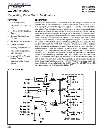
The UC1525A/27A, UC2525A/27A and UC3525A/27A are regulating pulse width modulator integrated circuits intended for switching power supply designs. The document lists features such as 8 to 35V operation, a 5.1V reference trimmed to ±1%, a 100Hz to 500kHz oscillator range, adjustable deadtime control, internal soft-start, pulse-by-pulse shutdown, and dual source/sink output drivers.
The datasheet provides absolute maximum ratings, recommended operating conditions, connection diagrams and pin functions, and electrical characteristics for the reference, oscillator, error amplifier, PWM comparator, shutdown and output driver sections. It also includes principles of operation, typical characteristics, shutdown options, oscillator and output circuit diagrams, and a lab test fixture.
| Supply Voltage (+VIN), Absolute Maximum | +40 V |
|---|---|
| Recommended Input Voltage (+VIN) | +8 V to +35 V |
| Reference Output Voltage (UC1525A/UC2525A) | 5.05 V min, 5.10 V typ, 5.15 V max at TJ = 25°C |
| Oscillator Frequency Range, Recommended | 100 Hz to 400 kHz |
| Output Current, Source or Sink, Absolute Maximum | 500 mA |
| Operating Junction Temperature | -55°C to +150°C |
| Packages | DIL-16 (J or N), PLCC-20 and LCC-20 (Q or L) |
| Reference Output Current, Absolute Maximum | 50 mA |
The recommended input voltage (+VIN) range is +8 V to +35 V.
At TJ = 25°C, the UC1525A/UC2525A reference output is specified as 5.05 V min, 5.10 V typ and 5.15 V max.
It immediately sets the PWM latch for fast turn-off and starts a 150µA current sink to discharge the external soft-start capacitor.
No; the text states Pin 10 should not be left floating because noise pickup could interrupt normal operation.