
UC1714/5 UC2714/5 UC3714/5 is a high performance driver with independently programmable delays that can provide drive waveforms for complementary switches. It can be used in synchronous rectifier circuits and active clamp/reset circuits.
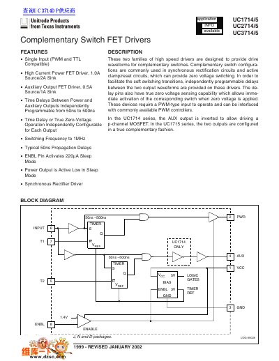
The document describes three families of high-speed driver circuits (UC1714/5, UC2714/5, and UC3714/5) designed to provide drive waveforms for complementary switches in synchronous rectification and active clamp/reset circuits. These devices feature independently programmable time delays between power and auxiliary outputs ranging from 50ns to 500ns.
| Supply Voltage (VCC) | 7 to 20 V |
|---|---|
| Auxiliary Driver Source Current (Peak) | 0.54A |
| Time Delay Range | 50ns to 500ns |
| Switching Frequency | to 1MHz |
The operating junction temperature range is -65°C to 150°C.
The device enters sleep mode, and the power output becomes active low.
Yes, the delay pins have true zero voltage sensing capability to activate switches immediately when zero voltage is applied.