
The MM70C95, MM80C95, MM70C97, and MM80C97 are monolithic complementary MOS (CMOS) integrated circuits constructed with N- and P-channel enhancement mode transistors. They convert CMOS or TTL outputs to TRI-STATE outputs with no logic inversion and provide the logical opposite of the input signal. The MM70C95 and MM80C95 and the MM70C96 and MM80C96 have common TRI-STATE controls for all six devices. The MM70C97 and MM80C97 and the MM70C98 and MM80C98 have two TRI-STATE controls, one for two devices and one for the other four devices. Inputs are protected from damage due to static discharge by diode clamps to VCC and GND. These gates have a wide supply voltage range (3.0V to 15V), guaranteed noise margin (1.0V), high noise immunity (0.45 VCC (typ.)), and TTL compatibility. They can drive 1 TTL load and are used in bus drivers. The typical propagation delay into a 150 pF load is 40 ns.
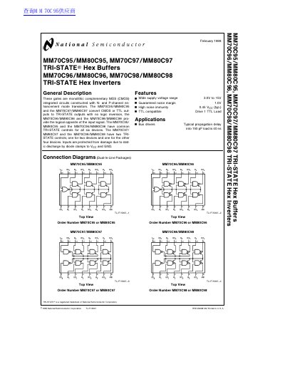
This document is a datasheet for the National Semiconductor MM70C95, MM70C96, MM70C97, and MM70C98 series of TRI-STATE Hex Buffers and Inverters. These monolithic complementary MOS (CMOS) integrated circuits are designed to convert CMOS or TTL outputs to TRI-STATE outputs. The devices offer a wide supply voltage range from 3.0V to 15V and are TTL compatible.
| Supply Voltage Range | 3.0V to 15V |
|---|---|
| Operating Temperature Range (MM70CXX) | -55°C to +125°C |
| Operating Temperature Range (MMB80CXX) | -40°C to +85°C |
The devices support a wide supply voltage range from 3.0V to 15V.
Yes, the datasheet lists TTL compatibility as a key feature.
The operating temperature range for the MM70CXX series is -55°C to +125°C.