
National Semiconductor MM54C89/MM74C89 64-Bit TRI-STATE handbook

This file is the English manual for MM54C89/MM74C89 64-Bit TRI-STATE Random Access Read-Write Memory
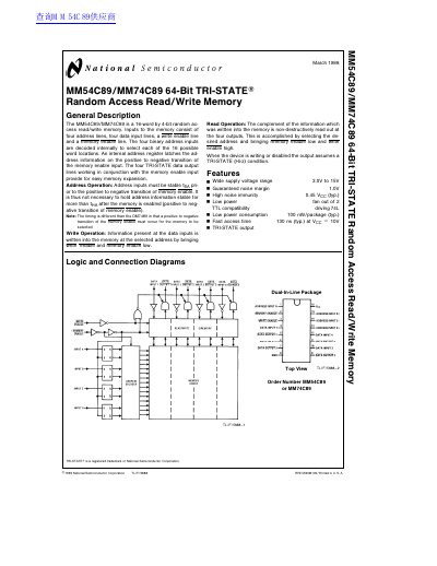

National Semiconductor MM54C89/MM74C89 64-Bit TRI-STATE handbook - cover page
Brand
National Semiconductor
Category
Memory
Document type
Datasheet
Language
English
Pages
6
File format
PDF
File size
131 KB
Published
07 August, 2012
Updated
30 September, 2023
MD5 checksum
4F689BF6B6AEB95BB1B42A08216204FE

About this manual

This document describes the MM54C89/MM74C89, a 16-word by 4-bit random access read/write memory. The device features four address lines, four data input lines, a write enable line, and a memory enable line to select word locations and latch address information.

What's inside

  • General Description
  • Features
  • Logic and Connection Diagrams
  • Absolute Maximum Ratings
  • DC Electrical Characteristics
  • AC Electrical Characteristics
  • Truth Table
  • Switching Time Waveforms
  • Physical Dimensions

Specifications

Memory Size16-word by 4-bit
Operating Voltage Range3.0V to 15V
Operating Temperature (MM54C89)-55°C to +125°C
Operating Temperature (MM74C89)-40°C to +85°C
Power Dissipation (Dual-In-Line)700 mW
Access Time Typ.350 ns @ 5V, 130 ns @ 10V

Frequently asked questions

What is the memory configuration of the MM54C89/MM74C89?

It is a 16-word by 4-bit random access read/write memory.

How are addresses latched in the device?

An internal address register latches the address information on the positive to negative transition of the memory enable input.

What condition do outputs assume when writing or disabled?

The output assumes a TRI-STATE (Hi-z) condition.

Download PDF (131 KB)

More National Semiconductor Manuals


View all National Semiconductor manuals →