
This document describes the features and characteristics of the TLF5881 MM54C32 and MM74C32 Quad 2-Input OR Gates. These gates employ complementary MOS (CMOS) transistors to achieve low power and high noise margin. They provide the basic functions used in the implementation of digital integrated circuit systems. The N- and P-channel enhancement mode transistors provide a symmetrical circuit with output swings essentially equal to the supply voltage, resulting in high noise immunity over a wide supply voltage range. No DC power other than that caused by leakage current is consumed during static conditions. All inputs are protected against static discharge damage.
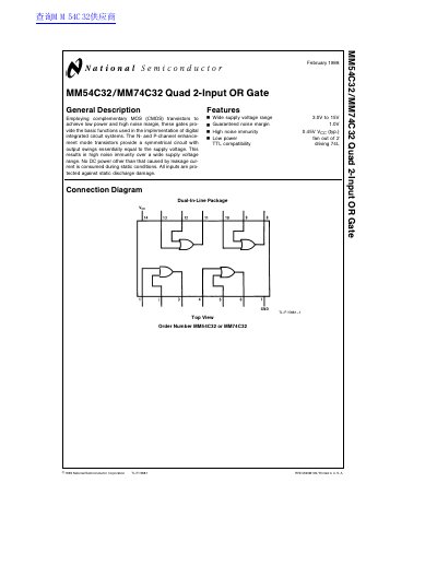
This document is a technical datasheet for the National Semiconductor MM54C32 and MM74C32 Quad 2-Input OR Gates. The devices employ complementary MOS (CMOS) transistors to achieve low power consumption and high noise immunity over a wide supply voltage range of 3.0V to 15V.
The datasheet provides absolute maximum ratings, DC electrical characteristics for CMOS-to-CMOS and CMOS/LPTTL interfaces, AC propagation delay times, and physical dimensions for both Dual-In-Line (J) and Molded Dual-In-Line (N) packages.
| Supply Voltage Range | 3.0V to 15V |
|---|---|
| Storage Temperature Range (Military) | -65°C to +150°C |
| Operating Temperature Range (Commercial) | -40°C to +85°C |
| Propagation Delay Time (Vcc = 10V) | 35 ns Typ / 70 ns Max |
| Input Capacitance | 5 pF |
The Dual-In-Line package has a maximum power dissipation of 700 mW.
The absolute maximum supply voltage is 18V.