
This document discusses the importance of PCB layout optimization and the factors influencing protection circuit design. By choosing the right protection location and suitable protection devices, interference issues in the circuit can be effectively addressed.
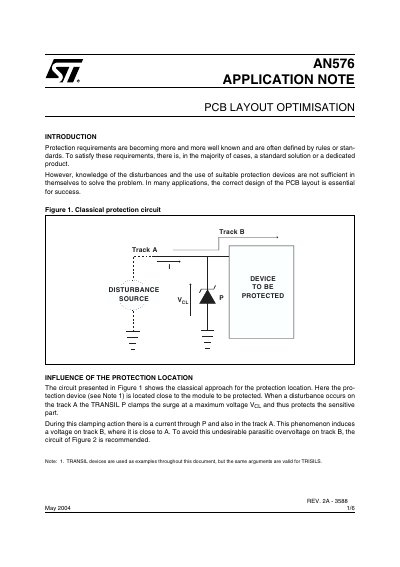
The document discusses standard protection requirements and highlights that correct PCB design is essential for success. It introduces a classical protection circuit where the device is located close to the module to be protected.
It then recommends an optimized layout where the protection device is placed as close as possible to the disturbance source, such as at the connector. This approach prevents parasitic overvoltages on adjacent tracks caused by high di/dt effects during clamping.
The protection device should be located as close as possible to the disturbance source.
High di/dt generates overvoltages in parasitic inductances between the protected points and the device, which adds to the clamping voltage.
A bidirectional Transil (BZW04P37B) is recommended between the printed circuit board ground and the metallic parts of the case.