
This document introduces the features of ADSP-2104/ADSP-2109, including 16-bit fixed-point DSP microprocessors, On-Chip memory, Enhanced Harvard Architecture, Independent Computation Units, Single-Cycle Instruction Execution & Multifunction Instructions, On-Chip Program Memory RAM or ROM & Data Memory RAM, Integrated I/O Peripherals: Serial Ports and Timer.
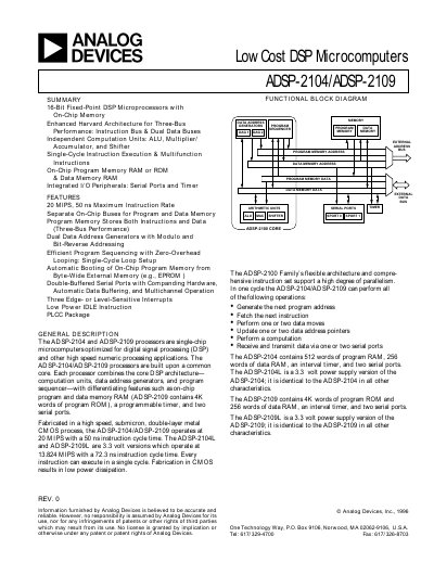
This document is a technical datasheet for the ADSP-2104 and ADSP-2109, which are single-chip microcomputers optimized for digital signal processing. These processors utilize an enhanced Harvard architecture with three-bus performance, independent computation units (ALU, Multiplier/Accumulator, Shifter), and on-chip program or data memory.
The datasheet details the functional block diagram, system interface requirements including clock signals and reset logic, and specific pin configurations for the 68-lead PLCC package. It also provides comprehensive electrical specifications, timing parameters, and ordering information for both standard voltage (5V) and low power (3.3V) versions of the chips.
| Maximum Instruction Rate | 20 MIPS |
|---|---|
| Instruction Cycle Time (Standard) | 50 ns |
| Instruction Cycle Time (Low Power) | 72.3 ns |
| Program Memory (ADSP-2104) | 512 words RAM |
| Data Memory (ADSP-2104) | 256 words RAM |
| Program Memory (ADSP-2109) | 4K words ROM |
| Data Memory (ADSP-2109) | 256 words RAM |
| Package Type | PLCC |
The ADSP-2109 contains factory-programmed on-chip ROM program memory (4K words), whereas the ADSP-2104 uses on-chip RAM.
Standard versions operate at 5V, while low power versions (ADSP-2104L/ADSP-2109L) operate at 3.3 volts.