
ADN2819/ADN2811 are multirate limiting amplifiers and clock and data recovery ICs with adjustable slice level. They integrate limiting amplifiers, clock and data recovery, and diagnostic functions. The ADN2819 supports multi-rate operation up to 2.7 Gbps, while the ADN2811 supports 2.5/2.7 Gbps data rates only. They exceed all SONET/SDH jitter requirements under all operating conditions.
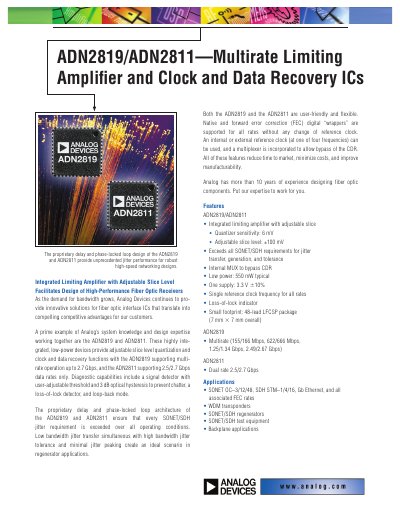
The Analog Devices ADN2819 and ADN2811 are highly integrated, low-power devices designed to provide adjustable slice level quantization and clock and data recovery functions. The proprietary delay and phase-locked loop architecture ensures that every SONET/SDH jitter requirement is exceeded over all operating conditions.
These ICs support native and forward error correction (FEC) digital wrappers for various rates without changing the reference clock. They feature an internal or external reference clock capability, a multiplexer to bypass the CDR, and diagnostic capabilities including signal detection with user-adjustable thresholds and loss-of-lock indicators.
| Quantizer sensitivity | 6 mV |
|---|---|
| Adjustable slice level | +100 mV |
| Typical power consumption | 550 mW |
| Supply voltage | 3.3 V +10% |
| Package type | 48-lead LFCSP |
The ADN2819 supports multirate operation up to 2.7 Gbps.
The typical low-power consumption for both models is 550 mW.
The devices require a single supply of 3.3 V with a +10% tolerance.