
MC100LVE210 is a low voltage, low skew dual differential ECL fanout buffer designed with clock distribution in mind. The device features two fanout buffers, a 1:4 and a 1:5 buffer, on a single chip. The device features fully differential clock paths to minimize both device and system skew. The dual buffer allows for the fanout of two signals through a single chip, thus reducing the skew between the two fundamental signals from a part–to–part skew down to an output–to–output skew. This capability reduces the skew by a factor of 4 as compared to using two LVE111’s to accomplish the same task. The MC100LVE210 works from a –3.3V supply while the MC100E210 provides identical function and performance from a standard –4.5V 100E voltage supply. For applications which require a single–ended input, the VBB reference voltage is supplied. For single–ended input applications the VBB reference should be connected to the unused CLK input of a differential pair and bypassed to ground via a 0.01µf capacitor. The input signal is then driven into the selected CLK input. To ensure that the tight skew specification is met it is necessary that both sides of the differential output are identically terminated, even if only one side is being used. In most applications all nine differential outputs are connected to 50Ω resistors to provide electrical termination.
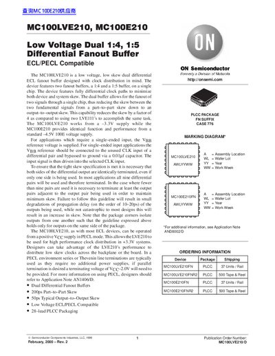
The MC100LVE210 and MC100E210 are low voltage, low skew dual differential ECL fanout buffers designed for clock distribution applications. The device integrates two fanout buffers on a single chip: one 1:4 buffer and one 1:5 buffer. These devices feature fully differential clock paths to minimize both device and system skew.
| Supply Voltage (LVE210) | -3.0V to -3.8V |
|---|---|
| Supply Voltage (E210) | -5.25V to -4.2V |
| Part-to-Part Skew (Diff) | 200 ps Max |
| Within-Device Skew | 50 to 75 ps Typ/Max |
| Output Rise/Fall Time | 200 to 600 ps |
The minimum input differential voltage required to produce full ECL levels at the output is 50 mV.
Yes, the MC100LVE210 can be operated from a positive VCc supply in PECL mode for use in +3.3V systems.