
SN54ABT16657 and SN74ABT16657 are 16-bit transceivers with parity generators/checkers and 3-state outputs. They feature state-of-the-art EPIC-ΙΙB BiCMOS design that significantly reduces power dissipation and exceeds JEDEC standard JESD-17 latch-up performance. The products have distributed VCC and GND pin configuration to minimize high-speed switching noise. They utilize a flow-through architecture for optimized PCB layout. The high-drive outputs (–32-mA IOH, 64-mA IOL) provide strong output capabilities. Package options include plastic 300-mil Shrink Small-Outline (DL) and Thin Shrink Small-Outline (DGG) packages, as well as 380-mil Fine-Pitch Ceramic Flat (WD) package with 25-mil center-to-center spacings.
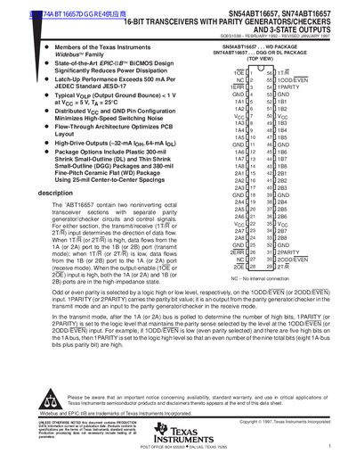
This document describes the SN54ABT16657 and SN74ABT16657, which are 16-bit transceivers containing two noninverting octal transceiver sections with separate parity generator/checker circuits. The devices feature state-of-the-art EPIC-II BiCMOS design to reduce power dissipation and include distributed VCC and GND pin configurations to minimize switching noise.
| Operating temperature (Military) | -55°C to 125°C |
|---|---|
| Operating temperature (Commercial) | -40°C to 85°C |
Odd or even parity is selected by a logic high or low level, respectively, on the 1ODD/EVEN (or 2ODD/EVEN) input.
The SN54ABT16657 is characterized for operation over the full military temperature range of -55°C to 125°C.
The SN74ABT16657 is characterized for operation from -40°C to 85°C.