
The SN54ABT16952 and SN74ABT16952 are 16-bit registered transceivers with 3-state outputs. They feature state-of-the-art EPIC-ΙΙB BiCMOS design that significantly reduces power dissipation. The latch-up performance exceeds 500mA per JEDEC Standard JESD-17. The typical VOLP (Output Ground Bounce) is less than 1V at VCC = 5V, TA = 25°C. The distributed VCC and GND pin configuration minimizes high-speed switching noise. The flow-through architecture optimizes PCB layout. The outputs have high-drive capability (-32mA IOH, 64mA IOL). Package options include plastic 300-mil shrink small-outline (DL) and thin shrink small-outline (DGG) packages, as well as a 380-mil fine-pitch ceramic flat (WD) package with 25-mil center-to-center spacings.
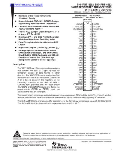
The document details the SN54ABT16952 and SN74ABT16952 devices, which are 16-bit registered transceivers containing two sets of D-type flip-flops for temporary data storage. These components support bidirectional data flow between A and B buses on a low-to-high clock transition when enabled.
| Operating Temperature (SN54ABT16952) | -55°C to 125°C |
|---|---|
| Maximum Clock Frequency | 150 MHz |
The SN54ABT16952 operates from -55°C to 125°C, while the SN74ABT16952 operates from -40°C to 85°C.
The devices support a maximum clock frequency of 150 MHz.