
This document describes the features and characteristics of the D2010UK power dissipation, drain-source breakdown voltage, gate-source breakdown voltage, drain current, storage temperature, and maximum operating junction temperature produced by Semelab plc. The product is a gold metallized multi-purpose silicon DMOS RF FET with a power dissipation of 83W, a drain-source breakdown voltage of 65V, a gate-source breakdown voltage of ±20V, a drain current of 8A, a storage temperature range of -65 to 150°C, and a maximum operating junction temperature of 200°C. It is suitable for VHF/UHF communications from 50 MHz to 1 GHz, with features such as simplified amplifier design, suitable for broad band applications, low Crss, simple bias circuits, low noise, and high gain.
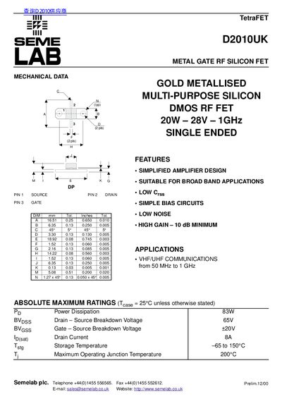
The Semelab D2010UK is a TetraFET Metal Gate RF Silicon FET designed for single-ended applications. It features a simplified amplifier design suitable for broad band applications, offering low noise and high gain of at least 10 dB. The device operates with a power dissipation of 20W, a drain-source breakdown voltage of 65V, and a frequency range from 50 MHz to 1 GHz.
| Power Dissipation | 20W |
|---|---|
| Common Source Power Gain | 10 dB minimum |
| Operating Frequency Range | 50 MHz to 1 GHz |
| Thermal Resistance Junction — Case | 2.1°C /W |
The device provides a high gain of at least 10 dB.
Yes, it is suitable for broad band applications with simplified amplifier design.