
These devices are high speed hex buffers with 3-state outputs. They are organized as single 6-bit or 2-bit/4-bit, with inverting or non-inverting data (D) paths. The outputs are designed to drive 15 TTL Unit Loads or 60 Low Power Schottky loads when the Enable (E) is LOW. When the Output Enable (E) is HIGH, the outputs are forced to a high impedance “off” state. If the outputs of the 3-state devices are tied together, all but one device must be in the high impedance state to avoid high currents that would exceed the maximum ratings. Designers should ensure that Output Enable signals to 3-state devices whose outputs are tied together are designed so there is no overlap.
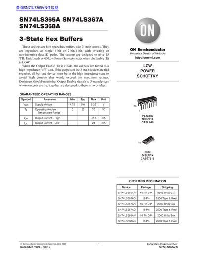
The document describes three related devices: the SN74LS365A (Hex 3-State Buffer with Common Enable), the SN74LS367A (Hex 3-State Buffer with Separate Enable sections), and the SN74LS368A (Hex 3-State Inverter Buffer). These high-speed hex buffers feature 3-state outputs designed to drive up to 15 TTL Unit Loads or 60 Low Power Schottky loads when enabled.
The datasheet details guaranteed operating ranges including supply voltage, temperature limits, and output currents. It provides DC and AC characteristics such as propagation delay times, input/output voltages, and power supply current under specific test conditions. Additionally, the document includes truth tables for logic operation and mechanical drawings with dimensions for the available 16-pin DIP and SOIC packages.
| Supply Voltage (Voc) | 4.75 V to 5.25 V |
|---|---|
| Operating Ambient Temperature (Ta) | 0 °C to 70 °C |
| Output Current - High | -2.6 mA |
| Output Current - Low | 24 mA |
The maximum output current is -2.6 mA for high states and 24 mA for low states.
The guaranteed operating ambient temperature range is from 0 °C to 70 °C.